https://jlcpcb.store/blogs/blog-post.atomJLCPCB - Blog Post2023-08-10T11:47:58+08:00JLCPCBhttps://jlcpcb.store/blogs/blog-post/regulator-and-other-heating-components-cooling-techniques-with-easyeda-x-jlcpcb2023-08-10T11:47:58+08:002023-08-10T11:47:59+08:00Regulator and Other Heating Components Cooling Techniques with EasyEDA x JLCPCBJLCPCB_Engineer
JLCPCB: There may be some components that generate high heat, such as the regulator, on the PCB. In order to prevent these components from being damaged, I am explaining PCB cooling techniques for you via EasyEDA ofJLCPCB. Especially if your circuit has to be fed with 12V and you are doing things that will draw a little more current with a 5V regulator, you will notice that your regulator gets very hot. You want to prefer an SMD regulator in your circuit. No problem. If you are not going to draw more than 400mA current, I am sharing a few circuit tricks for you. In this article, I will not go into technical calculations for the sake of appealing to everyone. I will just tell you the methods. If you really want an article that includes technical calculations, you can let theJLCPCBteam know. I will also prepare that article for you.
There may be some components that generate high heat, such as the regulator, on the PCB. In order to prevent these components from being damaged, I am explaining PCB cooling techniques for you via EasyEDA of JLCPCB.
Especially if your circuit has to be fed with 12V and you are doing things that will draw a little more current with a 5V regulator, you will notice that your regulator gets very hot. You want to prefer an SMD regulator in your circuit. No problem. If you are not going to draw more than 400mA current, I am sharing a few circuit tricks for you.
In this article, I will not go into technical calculations for the sake of appealing to everyone. I will just tell you the methods. If you really want an article that includes technical calculations, you can let the JLCPCB team know. I will also prepare that article for you.
1. A Regulator-Specific Tactic
First of all, we need to know that voltage regulators stabilize the voltage by converting excess energy into heat.
For example, let's say we have a regulator that reduces the 12V input to 5V. Let's say our circuit draws 500mA current. The regulator will need a voltage drop of 12V-5V=7V. Since the current flowing into the circuit through the regulator will be 500mA, 7V × 500mA=3.5W excess power will be converted into heat by the regulator. This creates a very high heat and requires a large heatsink aluminum plate or fan. Now JLCPCB will have a few tricks for you.
Did anything catch your attention? Since we cannot change the current drawn by the circuit, the greater the difference between the supply voltage of the regulator and the output voltage, the higher the power to be converted into heat will be. In that case, if we reduce the voltage difference to the minimum level before the regulator, the regulator will not overheat.
We can use diode for this. Generally, the supply voltage of 5V regulators should be minimum 7.5V. You can check this from the regulator's datasheet. We can reduce the 12V voltage to 7.8V by placing 6 silicon diodes (holding 0.7V voltage on the silicon diode) between the 12V voltage and the Vin pin of the regulator. There are two issues that we should pay particular attention to here. First, it is necessary to choose a good diode so that the diodes do not overheat or burn when they carry this current. The second is that we did not accidentally choose a low voltage holding germanium diode. Because these diodes will not hold 0.7V voltage, the calculations will be wrong. If your circuit draws too much current and the silicon diodes holding 0.7V cannot withstand the current, you can spread the heat over more diodes by using 15 germanium diodes holding 0.3V voltage instead.
2. Using the PCB as a Heatsink
Placing heatsinks on components often means extra workload and extra cost. You can use the PCB as a heatsink instead. In order to apply this method, you should pay attention to the package when choosing the component. It is very useful to have a heatsink surface that is in contact with the PCB surface as in the picture below. I will discuss this issue in more detail in Chapter 4.
A component with a cooling surface
You can find these components in JLCPCB's Assembly Parts Library. If you create a large copper area on the heatsink surface of the component as you can see in the picture below, the heat generated will spread over the PCB. So the component will cool faster.
A regulator cooling by PCB copper area
Let's look at how we created this copper field in EasyEDA of JLCPCB. As seen in the picture below, we first click on the option to create the copper field. Then, from the drop-down menu, we select Net to which the heatsink pin of the component is connected. (You can find which pin the cooler surface is connected to from the component's datasheet.)
Adding heatsink copper area to PCB with EasyEDA of JLCPCB
We draw the boundaries of the cooling copper area that will form around the component. (Avoid long thin drawings. Try to draw a border as close to the square as possible. Take care not to have different components within the borders you have drawn. A path passing through the cooler area may cause the cooler area to not work. Below you can see the incorrect and correctly applied cooler areas.)
Examples of correct / incorrect cooling with PCB copper area
Great. We created a cooling area for the component. Now let's make this area more effective with a simple trick. We create the same area that we have determined at the back of the circuit. Then, we add plenty of vias (jumping holes) to this area so that the heat can pass well behind the circuit. Of course EasyEDA will do this for us automatically.
Let's take a step-by-step look at how this is done with EasyEDA of JLCPCB.
Creating a double-layer heatsink copper area with EasyEDA of JLCPCB / Step 1
Creating a double-layer heatsink copper area with EasyEDA of JLCPCB / Step 2
Creating a double-layer heatsink copper area with EasyEDA of JLCPCB / Step 3
Creating a double-layer heatsink copper area with EasyEDA of JLCPCB / Step 4
Creating a double-layer heatsink copper area with EasyEDA of JLCPCB / Step 5
Creating a double-layer heatsink copper area with EasyEDA of JLCPCB / Finish
We now have a good cooler area. We can use the same methods for the pads of the diodes.
Cooling of voltage step-down diodes with wide copper paths in EasyEDA of JLCPCB.
3. Component Selection
In order for our cooler area to work well, the component we will choose should have plenty of contact with this area. That's why choosing the right component is important. You can easily meet your component needs from the JLCPCB Assembly Parts Library. You can also see their prices and compare them with equivalent products and add them to your circuit instantly with the product code. You can see the stock status and create your order with one click, including assembly, without any extra action. From the picture below, you can see the regulators that we should and should not choose for cooling from the Assembly Parts Library of JLCPCB.
Finally, you can see a regulator circuit prepared with the techniques in this article below.
A regulator circuit with a heatsink copper area designed in EasyEDA of JLCPCB using the techniques in the article
Stay tuned for more technical information and tricks.
Note: The methods described in this article make the heated components in your circuit less warm, but since this article does not include technical calculations, the methods described here are not guaranteed to protect your circuit against heat.
]]>
https://jlcpcb.store/blogs/blog-post/jlcpcb-metal2023-08-10T11:47:54+08:002023-08-10T11:47:54+08:00JLCPCB metal 3D printing keyboardJLCPCB_Engineer
JLCPCB: This time, as I announced at the end of the second article, I will summarize the details of the case production by JLCPCB metal 3D printing.We also changed the shape of the PCB, so we will also touch on the points to note when ordering.
]]>
About the case design
This is the design of the case that will be produced by JLCPCB metal 3D printing.
Some parts such as the protrusion on the inside are different from the final shape.
Last time I made a case which was made by resin, I was personally concerned about the thickness of the bezel width, so this time I tried to make the bezel as thin and slim as possible. In addition, the mounting method has been changed to reduce the height of the entire keyboard. As the result, it became as integrated shape with only the bottom, not the top and bottom split case.
As I wrote my previous article, my ultimate goal is to manufacture the case by cutting aluminum, so I designed it with an awareness of the shape that can be cut. However, with 3D printing, the price varies depending on the volume of the output, so we adjust the shape of the order data by removing parts that have no functional problems.
Futhermore, due to budget constraints, we decided to open the bottom part and cover it with FR-4 (glass epoxy, the meterial used for circuit boards). If you print the bottom, the price will more than double, so I took the plunge and remove this part. The change to this frame shape will becomea problem later, but it will be described later.
Cover with a bottom plate made of FR-4 without printing on the bottom
Flat switch plate and case top for easy cleaning
The front (right side of the image) is 12mm in height and thinned as much as possible.
Board design change due to change in mounting method
The previous resin case used urethana foam and a gasket mount that fixed the FR-4 switch plate between the upper and lower cases.
For the reason, the outer shape of the switch plate had "ears", but this time, the mounting method has beem changed to a fixing method like an O-ring mount, so the ears for the sandwiching are no longer necessary.
Regarding the change in shape due to the fact that the ears of the switch plate are no longer needed, we will not reorder the PCB, but will cut the perviously ordered FR-4 switch plate with a cutter and file the cross section. Acutally when I first placed the order, I decided on the shape, including the screw holes, so that I could try out several mounting methods, so this time it's a living form.
After removing the ears with an acrylic cutter, the end face was prepared with a file.
The PCB of the main unit also has a shape change. Since the previous case had a certain thickness in thee bezel, the PCB protruded the USB connector part in a convex shap.
Because the bezel was thick, the board shape of the connector part was made convex
This time, the bezel is thin and the PCB is inserted from the top of the case, so it is necessary to eliminate this convex shop. *If there is a protrusion, it will interfere when inserting from the top of the case & it is necessary to dent the shape inside the case.
This time, the PCB is inserted from the top side of the case, so it is changed to a flat shape so as not to interfere.
Change MCU to ATmega32U-MU
Although it is not directly related to his case shape change, the MCU has been changed from ATmega32U- AU to ATmega32U-MU. Although the ATmega32U-AU and ATmena32U-MU are functionally equivalent parts, they have no following differenes.
MU(7mm*7mm) has a smaller component size than AU(10mm*10mm)
MU has no soldering legs, so it is difficult to solder by hand.
The unit price of JLCPCB's PCBA service is overwhelmingly cheaper than AU. AU about $20, MU about $4
Actually, I was planning to order and mount the PCBA with ATmega32U-MU for the first board order, but when I ordered it, JLCPCB ran out of stock. So I changed the design data in hurry and made ATmega32U-AU by myself. Changed to the soldering policy. The inventory was revived when i was reordered, so I restored the design data again.
Precautions when ordering PCB boards
In this order, I tried decorating the board, but when I uploaded the Gerber data on the order screen of JLCPCB, I was puzzled by the preview being displayed with the black resist on the right side(back side) disapperaing. I thought that the design data was incomplete, so I changed the data serveral times and uploaded it, but the same phenomenon occurred. *The center of the surface on the left side of the image is circular and yellow, which is the correct state.
In the preview, the resist on the back side has disappeared, but if you check the Gerver Viewer on the lower right...
However, when I open JLCPCB's Gerber file Viewer and checked it, I noticed that the resist layer was hidden. I don't know the detailed cause, but this kind of phenomenon occurred when the Cu(copper foil) layer was arranged in a fine shape all over.
For some reason the registration layer was unchecked
If you check it, it will look correct
Just in case, enable layer display on Gerber Viewer. The preview image on the ordering screen did not change even if layer display was enabled, but I was able to confirm that there was no problem with the data, so I placed the order in this state.
I will post pictures of the actual product later, but the board I received was as designed and there were no problems. However, depending on the order data, the preview may be correct(the order data is incorrect), so if you cannot solve the problem or are worried, it may be a good idea to contact us!
Ordering JLCPCB metal 3D printing and correcting data
Now for the JLCPCB metal 3D print order for the main case. After uploadinf the design data optimized for 3D printing, the engineer in charge of comfirming the data contacted me that the output might be distorted. I received the same message when I printed out the rsein, and I replied thhar some distortion was acceptable, so please print out the data as it is, and I started the production procedure.
However, after that, we received another concern from the factory engineer that this frame-like shape was expected to cause a large amount of distortion. At this point, I understand that the distortion is not tolerable, so U canceled the order.
Consideration for the cause of distortion
According to the engineer, the bottom part os small and has a frame shape, so there is a cconcern that the output will shrink toward the center (or spread in the opposite direction). In the laser melting method(SLM), which melts and solidifies stainless steel powder with a laser, the modeled object is slightly distorted due to the temperature difference between the hot part and the cold part. There are similar concerns with resin output of stereolithigraphy, but in this case of metal printing, the temperature due to laser irradiation is so high that it cannot be compared with resin, so if the shape is not appropriate, the distortion will increase. *If the shape is appropriate, it is an output method that gives very high accuracy.
From here on, it's just my guess, but another possible cause of excessive distortion is the output direction of the modeled object.
JLCPCB's metal 3D printer has an output area of 250x250x300mm. Since the long side of this case exceeds 250m, it must be installed in one of the following two direction with respect to the stage.
Vertical placement with the right of left side of the case facing down
The long side of the USB connector (rear) side is grounded diagonally to the stage.
In either installation method, the installaton area for the stage is small, and the bottom opening is free for printing. I am assuming that is what causes the distortion. Perhaps there is some twisting in addition to the contraction toward the center.
Even in the second installation direction, the open part of the bottom is output in a free state, so it is distorted
Respond by correcting the data
The best solution is to print the bottom part with appropriate thickness without removing it, but I can't do that because I'm framed for budgets reasons.
As a final solution, I divided the frame shape into four parts and output each side as one part. After receiving eash side, cut the threads and combine them with set screws. By the way, the fee is calculated by the volume of the output product, so it doesn't change whether you divide it. Rather, it was a little cheaper for the lower hold of the screw.
back and front. Although it exceeds 250 mm, it can be output by arranging it diagonally to the stage.
side
The parts on each side are fixed with M3 setscrews and combined.
When I uploaded the data divided in this way again, this time the data was approved without any problems. The warning mark in this image is due to the fact that the diagonally divided part was judged to be thin.
Successfully passed manufacturing inspection
By the way, I thought that outputing a part with only one side might distort (warp) during modeling, so I upload the following data with two sides connected with support material just in case.
Data that joins the back and front parts with support material and makes it a cylinder as a whole
Data in which the sides are joined with support material
However, these didn't pass the manufacture inspection. This is because, as started in this JLCPCB print guideline, metal printing does not support printing multiple parts that are connected with support materials. Make sure you check the conditions beforehand.
Please kindly note: FDM with ABS material and SLM with 316L meterial are not supported in this way.
In the case of metal 3D printing, data with support material does not pass the manufacturing review
As a result, we settled on printing the parts on each side individually.
Manufacturing
Just when I thought that production had finally started, the following text was displayed on the order screen. It says that the delivery time will be longer than expected.
Audit failure reason, but message about late delivery
Recently, the production of SLM-316L material is under heavy load, the build time will be add 1-3 business day! Hope for your kind understanding! thanks!
As shown in the following video, even JLCPCB, which has a large number of 3D printers, only have one printer that can output metal. So this kind of thing will happen if orders overlap. Relax and wait.
After few days. the status changed to In Production and production started.
However, the display showing the progess of manufacturing stopped at the first step (Data Processing) for about two days, so I wondered if the engineer was busy and could not update the status for the web, but the display changed. I continued to wait patiently.
It seems that my prediction was correct, and the status suddenly changed to waiting for shipment, and I was notified that the production was completed. When manufacturing resin parts, the status was updated from time to time, so it seems good to know in advance that this may happen in the case of metal output products.
The next progress was updated and comfirmed after shipping notification was received.
You can see that the output work was done in Data Processing ~ Printing
Arrival of substrate after specification change
As for the JLCPCB metal 3D printing, we had to recreate the order data and as mentioned above, the delivery was delayed, so we received the board with the changed specification earlier. The following three types of board were ordered. *The board and the 3D printing cannot be shipped together.
Bottom plate x 2 types
PCB that becomes the main body of the keyboard
This time it's not the familiar blue box
Opened
I tried using the option to remove the order number, which I did not use in the previous order, and the option to have papper sandwiched to prevent scratches when delivering the board.
Please note that the option to insert paper cannot be used for boards that use PCBA because uneven parts are created (in the first place, it cannot be slected on the order screen).
Use the option to have the paper sandwiched to prevent scratches and the order number removal option
Boards using PCBA cannot use the option to sandwich paper
Copper foil (Cu layer) is used as one element for decoration, but it becomes silver (HASL wit Lead), silver (LeadFree HASL), and gold (ENIG) depending on the surface finish such as lead-free. ENIG is a process called electroless gold plating, and it's expensive, so I haven't tried it myself, but as far as I can see, it seems to be gold.
Experiment with decorative substrates using copper foil, resist, masks, etc.
The logo, which was silk-printed last time, is made brighter with copper foil this time (it's hard to understand because the photo is poor...)
The shape change of the USB connector part is also manufactured as intended.
Changed shape of USB connector
As shown in the following photo, the ATmega32U-MU has a much smaller component size than the ATmega32U-AU, so I think it will be an effective option for keyboards that do not have room for board component layout.
The bottom is ATmega32U-AU footprint, the top is ATmega32U-MU (installed). one size smaller
Arrival of JLCPCB 3D printed stainless steel case
This time, I wanted to receive it as soon as possible, so I used FedEx International Packet (delivered in 3-6days) instead of OCS Express (delivered in 4-8days). For comparison, the shipping cost was about $8 for OCS and about $15 for FedEx.
I received the delivery notice on 24/10 and arrived at hand on28/10. It was delivered to me by Yu-Pack as a domestic agent,
Regarding customs duty and comsumption tax, it seems that a payment form will be sent at a later date.
Shipped on Monday and arrived on Friday
Another layer was covered with packing material, preventing the model from moving.
Confirmation of model
Here is the sculpture I received.
It has a more solid and solid feel than I imagined, giving the impression of a lump of stainless steel. This 316L is called surgical stainless steel, and it is also used for jewelry because it is less prone to corrosion and rust and less likelty to cause metal allergies.
Almost no distortion to worry about
There was almost no distortion, which I was concerned about, and the printing was very accurate.
In the photom it's light gray, but in real life it's very cool because it's close yo the space gray colour in Apple's product lineup. I would probably polish the surface to give it a silvery sheen, but I like the darken tone of this matte so left it as is.
temporary assembly
Accuracy has been achieved, so it fits perfectly at the stage of temporary assembly
If it were made of aluminum, it would not be possible to put out this weight with this size due to the specific gravity.
In the case of metal 3D printing, electricaal discharge machining is used to separate the model from the stage (wire electrical discharge machining). As a result, the surface that was in contact with the stage during printing will have sawtooth marks as shown below. However, since the surface trreatment is applied after cutting, it does not have the impression of being rough, and it is relatively smooth.
oblique cut
It's hard to see, but there are traces of cutting parallel to the long side.
If it is installed at an angle to the stage, this mark will be slanted, and if it is installed at a right angle or horizontally, it will leave a mark of teeth that are perpendicular or horizontal to the modeled object.
The red straight line is the wire for cutting and the direction of travel. When placed diagonally on the stage, the cut marks remain diagonally
The other sides have a cast metal-like texture. Is it like this becuase the stainless steel powder is melted and solidified by the laser?
cast iron texture
The output mark remains diagonally, but it is an inner part, so it does not bother me
Additional work and assembly
After confirming each part, we will assemble it. Each side is assembled with M3 setscrews, and a bottom plate made of FR-4 is used to secure the entire frame for rigidity. As a piolt hole, a φ2.5 hole was provided in the ordering data, but the accuracy was perfect, so it was easy to cut the M3 tap.
I was worried because stainless steel is hard, but the tap cut easily
Combine with the M3 setscrew that was lying around at home
Sorry for the out-of-focus
Only 4 setscrews are used, which is the minimum required, so if you use only these screws, the entire frame will be loose. For thar reason, we combined it with two FR-f bottom plates, which are more accurate than 3D printing, to fix the entire frame and increase its rigidity.
The plates are attached together with double-sided tape.
Rubber feet on the bottom plate
The bottom plate and case are also fixed with double-sided tape. Also suitable for screwing
This completes the assembly of the case. With only 4 setscrews, it was wobbly, but by combining it with a plate, we were able to secure rigidity and it became ticking.
Top side (There are traces of double-sided tape on the inside of the back part)
bottom side
The weight has been increase by about 100g from the stainless steel parts alone, making it even heavier.
Plenty of weight for being thin and small
Combining the case and keyboard body
Next, we will combine the case and keyboard body.
This time, the internal structure is simplified to make it as thin as possible. Therefore, we designed a case that use an O-ring mount as a cape method. Nornally, an O-ring like the one shown below is wrapped around the outer circumference of the gap between the switch plate and the PCB of the keyboard body, and the keyboard body is fixed by friction between the O-ring and the case.
However, this time, when I happened to be wandering around a home center near my home, I found a super-cheap product called a mesh holding rubber ( a product for fixing the screen door to the frame). I thought that this could be an alternative to O-rings, so I bought it as a trial.
There are also variations in the diameter of the mesh holding rubber, so If you are using an acrylic switch plate or a low-profile keyboard, you may be able to use it.
This time, will will use Cherry MX compatible key switches, and since we are using a 1.6mm thick FR-4 switch plate, we will use 3.5mm diameter rubber.
Urethane foam is pasted on the top of the case to prevent the PCB from sinking too much.
The distance between the switch plate and the board body is 3.4 mm, but it can be easily wrapped around because it is crushed moderately.
If I would it as it is, the rubber would be crushed too much dur to its hollow structure. Therefore, I decided to wind a thick water string (kite string) lying around the house about 2 times to increase the volume, and then wrap the rubber on top.
Increase the volume with water thread so that the rubber is moderately exposed to the outside. The knot was in the way, so I cut it after this
Now the rubber protrudes moderately from the outer shape of the PCB and can be fixed to the case. They are evenlt spaced inside the case so they stay in place even when you type or turn them over. You can easily replace the key switch,
I haven't test yet, but it mat be possible to ground it to the case without the need to winf the string with a thick holding rubber such as 4.5mm or 5.5mm.
Complete keyboard "inn v2.1"
Here's an overview of the complete keyboard: the width of the bezel has also become thin to my liking, and I was able to eliminate the dissatisfaction of the previous case that led to the change. As for the colour of stainless steel, it is unexpectedlt very astringent, and I really like it.
The bezel is thin and refreshing
I want to try beige and dark color keycaps
The tilt angle is 3.4°. The first prototype was easy to use, so I adopted that angle as it is.
back
Bottom. The gap between the side parts is because the set screw on hand is too short and can not be tightened.
Impressions atfer completion
The case of this time is based on the size of the first prototype case made by processing aluminum angles. As a result, we achieved a significant increase in weight with almost the same size, and were able to acquire a sense of stability and rigidity.
The bottom is the very first prototype made with aluminum angle. very light
Personally, my ultimate goal is to manufacture a case by cutting aluminum, but if it is for personal use and not for sale, I feel that metal 3D printing is sufficient,
Above all, this compact keyboard has thin bezels and a low height, but the fact that it is so heavy due to its specific gravity has led to more satisfaction than I imagined. Unexpectedly, it was a discovery that if I made it with this design using machined aluminum, I might be dissatisfied with the weight.
Even with the same volume, stainless steel weighs about three times as much as aluminum.
This time, due to budget constraints, we used a frame-shaped case with an open bottom, so we had to print in separate pieces and assemble it. However, due to the output area, the limit is the diagonal size of the stage whose long side is 300 mm or 250 x 250 mm in the Z-axis direction, so if it is not divided, the limit may be about 65%.
If you are interested, why not try making a case with JLCPCB metal 3D printing?
JLCPCB, where I made PCB and 3D printed this time, also distributes $54 new user coupons!
]]>
https://jlcpcb.store/blogs/blog-post/what-is-a-docupling-capacitor-and-how-is-it-placed-with-easyeda-x-jlcpcb2023-08-10T11:47:35+08:002023-08-10T11:47:35+08:00What Is a Docupling Capacitor and How Is It Placed With EasyEDA x JLCPCBJLCPCB_Engineer
JLCPCB: Filter circuits are used in many designs. Especially in circuits where the signal lines are carried by a long cable, fluctuations caused by the magnetic field outside should be filtered. These fluctuations can cause false signal detection and even break the processor with very high fluctuations. Generally, filters containing capacitors are used to prevent such situations. Because capacitors can absorb sudden surges on themselves. Capacitors used in filter circuits are simply called filter capacitors. But there is also a type of capacitor called a decoupling capacitor. Here we will see with examples what this capacitor does and how to place it withEasyEDA,JLCPCB's PCB design tool.
Filter circuits are used in many designs. Especially in circuits where the signal lines are carried by a long cable, fluctuations caused by the magnetic field outside should be filtered. These fluctuations can cause false signal detection and even break the processor with very high fluctuations.
Long-Wire Signal Line Filtering
Generally, filters containing capacitors are used to prevent such situations. Because capacitors can absorb sudden surges on themselves.
Capacitors used in filter circuits are simply called filter capacitors. But there is also a type of capacitor called a decoupling capacitor. Here we will see with examples what this capacitor does and how to place it with EasyEDA, JLCPCB's PCB design tool.
1. What is Decoupling Capacitor?
In fact, the decoupling capacitor is also the same as standard capacitors. Due to its area of use, it has only received a special name. Because the only purpose of the decoupling capacitor is not to prevent fluctuations in the line, but also to protect an integrated. For this, the placement of the capacitor should be as close to the integrated as possible. It is selected at a value of approximately 10nF. The capacity value may vary depending on the situation.
A 10nF Capacitor From The JLCPCB Assembly Parts Library
You copy the JLCPCB Part Number of a capacitor you choose from here and open the Library section of JLCPCB's PCB design tool EasyEDA. You paste the copied JLCPCB part number here and add the resulting capacitor to your circuit.
Adding a Selected Component from the JLCPCB Assembly Parts Library to EasyEDA
The important thing here is the placement of this capacitor in the circuit. You should place this capacitor right next to the integrated we want to protect. Thus, even if the path is exposed to the magnetic field, a smooth current will enter the IC, with all fluctuations filtered before entering the full IC.
Remember, it's not enough to just filter a line from a remote point. While that line is traveling in the circuit, fluctuations may occur again by being affected by the magnetic fields formed in different ways. If you are not using a decoupling capacitor, these fluctuations will directly enter your IC.
Correct and Incorrect Positioning of a Decoupling Capacitor in EasyEDA, JLCPCB's Circuit Design Tool
2. Is Decoupling Capacitor Necessary?
Decoupling capacitor is not required. But its use is very beneficial in terms of integrated health.
The use of decoupling capacitors in the supply inputs of processors is a big plus in terms of circuits, especially in circuits with sensitive integrated circuits, circuits with sensitive measurement.
In addition, a decoupling capacitor in a 402 sheath with a value of about 10nF will not take up much space and can be easily added to many circuits. In EasyEDA, JLCPCB's PCB design tool, you can easily add this capacitor and simply protect your ICs.
3. Which Capacitor Type Would Be Best For Decoupling?
The best choice for decoupling capacitor will usually be small ceramic capacitors. Increasing the size and capacity of capacitors does not necessarily mean better filtering. Forget it. If you increase the capacitor's capacitance, you filter out lower frequency fluctuations. But the decoupling capacitor is especially used to filter out extremely high frequencies. I'm talking about frequencies above about 50 MHz.
Also, ceramic capacitors have a high temperature range. They have a wide voltage range and do a great job.
When choosing your decoupling capacitor, you can choose by considering them.
4. How Many Capacitors Should Be Used?
In most cases, the use of a single 10nF ceramic capacitor is sufficient. But your circuit may have too many high frequencies. There may be a lot of magnetic field in your circuit. You may be carrying high current in your circuit. A motor may be connected to your circuit and causing interference. In these cases, you may prefer to connect more than one decoupling capacitor in parallel.
Example of Multiple Decoupling Capacitors in EasyEDA, JLCPCB's Circuit Design Tool
Do not increase the value of the capacitor. This does not give you any more protection. Changes the frequency to be protected. You can use multiple 10nFs in parallel instead of increasing the capacitor value. If you have low-frequency interference in your circuit, you can also choose to parallel connect a smaller capacitor and a higher-capacity capacitor in parallel.
]]>
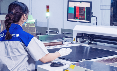
https://jlcpcb.store/blogs/blog-post/get-benefits-from-smt-assembly-jlcpcb2023-08-10T11:47:35+08:002023-08-10T11:47:35+08:00Get Benefits from SMT Assembly-JLCPCBJLCPCB_EngineerJLCPCB SMT technology allows fabrication yield. Compared with THT or hand soldering, SMT is more suitable for automated production. THT requires different insertion machines according to different components, each machine needs to adjust the assembly time, and the maintenance workload is large. SMT can install all types of SMC/SMD by using one placement machine with different feeders and pick-and-place pin, which reduces adjustment preparation time and maintenance workload. Compared with JLCPCB PCB assembly , hand soldering has a high risk of making defective boards. In addition to the solder paste printing machine, pick and placement machine, and reflow oven that needs to attach electronic components to the circuit board, the JLCPCB PCBA servicehas enough inspection equipment.
JLCPCB SMT technology allows fabrication yield. Compared with THT or hand soldering, SMT is more suitable for automated production. THT requires different insertion machines (DIP insertion machine, radial insertion machine, axial insertion machine, tape machine, etc.) according to different components, each machine needs to adjust the assembly time, and the maintenance workload is large. SMT can install all types of SMC/SMD by using one placement machine with different feeders and pick-and-place pin, which reduces adjustment preparation time and maintenance workload. Compared with JLCPCB PCB assembly , hand soldering has a high risk of making defective boards. In addition to the solder paste printing machine, pick and placement machine, and reflow oven that needs to attach electronic components to the circuit board, the JLCPCB PCBA service has enough inspection equipment.
Visible Difference:
White PCBA : This PCB is hand soldered, using the same components. ESP32 module is shorted due to too much solder between the two pins.
Black PCBA: It's a PCB soldered using the JLCPCB SMT service, the soldering is done professionally and the components are properly aligned.
Invisible Fault: Detached Pads on Component’s Bottom Side
The below board is showing PCBs with UVC LEDs assembled. These UVC LEDs have solder pads on the bottom side, like BGA. For the first prototyping, I used JLCPCB’s PCBA service, and the prototype worked well as it was designed.
Benefits of JLCPCB SMT Assembly
From hundreds of domestic users growing to nearly 100,000 SMT users globally now, more and more customers choose and benefit from JLCPCB SMT service. JLCPCB is at the forefront of the PCB manufacturing industry, we clearly solve the pain points of this industry and the needs of users. Especially this service can appropriately satisfy new products’ R&D. It really meets our needs. Engineers said that they can start their own business without worries because of JLCPCB. Features of JLCPCB SMT service:
The cheapest PCB/PCBA price and Competitive freight save your costs.
Integrated in-stock 350K+ JLCPCB Parts& 10 million+ global parts.
One-stop Manufacturing: from parts preparation and PCB production to PCB assembly, even to 3D printing can be realized at the same factory, in the shortest time.
How SMT ServiceSaves Engineers Money
JLCPCB sends every customer the $24 SMT coupon to enjoy PCB assembly service. Authentic components, high equipment, factories, professional technical teams to achieve engineers' real profits. JLCPCB has insisted on $2 for 5PCBs, an $8 PCB assembly setup fee, and 3D printing from $1
JLCPCB components price is transparent: PCB assembly components' price is clearly marked. Compare to buy-as-you-go mode, pre-order parts allow people to get a favorable price. Pre-order service adopts real-time quotation service, and the price is transparent and open. Customers can purchase on-demand without worrying about the loss of payment due to the failure of the pre-order service. JLCPCB is able to obtain more low-cost but high-quality parts from reliable global parts suppliers. The bargaining power of JLCPCB can help small and medium-sized enterprises or individual customers reduce cost risks, collect various component needs, and negotiate prices with trusted component suppliers.
Sourcing 350k+ in-stockparts& a Million Global Parts
JLCPCB has a large selection of components for PCBA orders to achieve 100% parts assembly.
In case the parts suddenly run out of stock when PCB assembly is needed, we provide the pre-order parts service based on the JLCPCB parts library. If the JLCPCB parts library still can't fulfill your PCBA order to get all parts assembled on your boards, we launched the global sourcing service that sources and stocks parts from JLCPCB and global distributors, like digikey, mouser, TI, etc.
Please note the parts pre-order service or global sourcing service is only for PCB assembly orders, the parts won't be shipped separately to you.
One-Stop Service Saves EngineerTime
Saving engineers time requires advanced factory and equipment. Self-operated factories are the primary condition to ensure high-efficiency SMT production lines. Self-operated factories can achieve quality control and mass production. At present, JLCPCB's 6 large self-operated factories have high-end equipment and professional technical teams to ensure stable production of 96 SMT production lines. 90% of SMT orders only take half a day of production: PCB, stencil, and components are produced in self-operated industrial centers, with guaranteed quality and delivery. In the JLCPCB factories, AGV is used to realize PCB production, no transfer is requested: component preparation, and stencil production until PCBA.
Time-saving SMT service for engineers requiring reliable one-stop PCB service from design to PCB enclosure:
PCB design, PCB fabrication, PCB assembly, and 3D printing realized on a one-stop platform
Standard PCB Assembly supports double-side soldering, and unlimited quantity, order as many as you want
JLCPCB SMT Parts Library 350k+ in-stock components ; and 10 Million+ global sourcing parts from reliable parts suppliers worldwide
Pre-Order from Global Reliable Parts Suppliers+Build Personal library Inventory
Technology brings high SMT technology, which avoids the harm from hand soldering, and allows engineers to have more energy to benefit human beings and enjoy more fun in life. Batch production can be handed over to JLCPCB. Its standardized independent online ordering method only takes 12 hours for assembly. Once the PCB file is approved, the delivery of PCB+SMT can be completed the next day.
Staying electronic engineers healthy
Chemical composition of rosin and tin wire, which is directly inhaled into electronic engineers' lungs. Cervical spondylosis is quite common for hand-soldering engineers. Takes hours to solder, which causes painful cervical spine , hooking neck and using hands-on small resistors and capacitors.SMT technology saves engineers time and keeps them away from chemicals as well as cervical spondylosis.
Be an SMT technology forerunner ——
Working on fully assembly & the highest parts auto-matching rate
JLCPCB SMT has always been committed to providing efficient, self-help service. The matching of orders is the highest frequency, and it is also the most critical technology to improve the efficiency of the effect. In 2021, JLCPCB set up a special project team to improve this automatic matching rate. They first created a system to measure whether the matching rate has indeed improved, and at the same time, we can quickly locate the problem of customer matching.
Case:
"We use the monitoring and debugging functions of our system, and we feel strange, according to the stock price, the package should match another C1525, how come it is C1608?"
"It is found that the matching of the diagnosis is the C number matching, and then when the customer contributes the customer number, we query the customer's BOM. The customer's library file is C1608, and we use C1608 first as the store's number."
JLCPCB spent time fixing compatibility issues with messy BOMs. To mine the product number, the success rate has been increased by 5%. It is difficult for technology to be beneficial to everyone, and they only speak with data. After 1 year of development, the auto-matching rate rose from 54% to 85%. Only 15% of parts need to be chosen by yourself when ordering PCBA on JLCPCB. Customers and salesmen have always been praised, and this matching rate also allows us to actively monitor problems.
SMT matching is still iterating, and JLCPCB will gradually improve it. It is estimated that JLCPCB SMT matching will increase by more than 6% points by the end of this month, which is estimated to be the highest level of matching rate in this industry.
Be engineers' best PCBA choice
Keeping an open mind and embracing every customer is the working attitude of JLCPCB. Customer opinions and feedback are the motors of the JLCPCB SMT project progress. Listening and communicating go both ways. JLCPCB serves 172 countries around the world, serving 1,000,000 +Customers, with higher than 99.97% On-time delivery, and lower than 0.23% Quality Complaint Rate. Remarks from PCBA customers:
JLCPCB has been committed to reducing PCB/PCBA costs, improving the ordering experience, and speeding up lead-time and shipping. Many entrepreneur customers said JLCPCB helps them to improve business through time and cost-saving.
"Besides PCB assembly, we like JLCPCB free gifts, packages, and people!" "Open the box on the top side . We have cardboard, some bubble wrap, another layer of bubble wrap and another roller wrap. You can see PCB wrapped in bubble wrap and not just cardboard has some foam inside and some more power wraps of damage during shipping it's almost impossible anyway"
In terms of the current performance, we would like to define JLCPCB SMT as a mode. SMT is no longer be a factory, but a connection in the production chain in the future. JLCPCB SMT remembers the original aim and will make every endeavor an extremely great customer experience. Saving your PCB assembly now and in the future, get JLCPCB $24 monthly SMT coupon!
]]>
https://jlcpcb.store/blogs/blog-post/jlcpcb-3d-printing-in-japan2023-08-10T11:47:35+08:002023-08-10T11:47:35+08:00JLCPCB 3D Printing in JapanJLCPCB_Engineer
JLCPCB is a Chinese company famous for manufacturing printed circuit boards.
You can order manufacturing PCB data created by KiCAD and other software by simply clicking on the web page, even from Japan The prices are quite reasonable, andJLCPCBis widely used among hobby electronics craft users. Also JLCPCBhas recently started a "3D printing service.
JLCPCB is a Chinese company famous for manufacturing printed circuit boards.
You can order manufacturing PCB data created by KiCAD and other software by simply clicking on the web page, even from Japan.
The prices are quite reasonable, and JLCPCB is widely used among hobby electronics craft users.
JLCPCB has recently started a "3D printing service.
So this time, I would like to introduce what this 3D printing service is like, using my actual order as an example.
Again, when ordering 3D printing from JLCPCB, I decided to use the following two types of data that I have created in the past.
Chassis of an electronic musical instrument called RakuChord
RakuChord - an electronic musical instrument that can be played like a RakuChord with ease.
Plate receptacle for the drainer shelf
Introduction of Kitchen Drainboard and Fixing Problems with 3D Printer - inajob's blog
One of the difficult parts of 3D printer is to design a suitable design for 3D printing, but in this case, I was able to skip this difficult part because of my past efforts.
Once the data is created, it can be created again and again, which is a convenient feature of 3D printing and other machining processes, unlike manual processing.
Ordering
Assuming that you have already registered as a JLCPCB user, we will introduce how to place an order on the web.
However, there is nothing difficult to do, just uploading the data.
Although JLCPCB is a Chinese company, the web service is written in English, so there is nothing particularly confusing.
Registration of order data
First of all, upload the STL file from the order page, which is a familiar feature of 3D printing, and the following screen will appear.
All you have to do is write the material, number of pieces, and description.
You can choose from a variety of resins and metals, but this time we chose the inexpensive SLA (Resin).
Furthermore, there are three different materials within that category, but the differences between these seem to be subtle, so for the large drainer shelf, I chose the cheapest, 9000R Resin.
The amount seems to be determined almost entirely by volume, and this draining rack was $16.49. (Note that the volume also affects the shipping cost.)
Product Desc is where you describe what it is. In this case, we chose to use "Kitchen tool".
Next is the RakuChord part. It is very inexpensive because it has only small parts in volume compared to the drainer shelf. The smallest screw part was only $1.0.
I selected different materials in the same SLA (Resin) for a test.
Shipping charges
The next step is to check the shipping costs.
There are a variety of shipping options: very slow but cheap, fast but expensive, etc.
This time we chose DHL, which is fast and slightly more expensive.
This is because I have experienced various problems when I usually use cheap carriers such as AliExpress, such as the shipment arriving really crudely packed, taking a month to arrive, or being damaged.
The shipping cost this time was $27.63 with DHL. (The lowest price I could find was $9.77 from Economic Global Direct Line.)
The larger the product, the larger the shipping cost will be, and I felt that no matter how low the production cost is, there will be cases where we lose money on shipping.
About the review
If you have done 3D printing before, you know that it is difficult to 3D print some shapes.
That's why JLCPCB has a manual (?) review process exists. When you Order your registered order data, you have to wait a little bit for the review process before payment.
In my case, the review was completed the next day.
I was warned that some parts were very thin and that this part might not come out correctly, but this time I chose to proceed (YES in the figure below).
Waiting
After placing the order, I waited for 6 days and the sculpture arrived at my home via DHL.
I personally felt that it was "fast" to receive an original molding designed by myself in 6 days.
About the workmanship (draining shelf)
I have been using a home-use (?) I was very impressed with the output of the optical 3D printer, as I had only handled a home 3D printer.
As for the drainer shelf, the simple shape and very 3D printer-friendly design made it possible to find no defects in the modeling process.
The dimensions were also matched with the 3D printer we already have at home, so we were able to start using it in our kitchen right away.
This may not be an appropriate comparison, but here is a comparison with the one made by our 3D printer (stacked type).
About the finished product (RakuChord)
This was also data that had been output with a stacked 3D printer at home, but it was a more complex shape than the drainer shelf, with many thin sections, making it a more difficult modeling from the 3D printer's point of view.
As expected, the thin, pointy corners were output with a slight warp, and I felt that even if a professional did it, this could still happen.
Well, the warpage is acceptable for my application, but it seems to be difficult to make it exactly according to the data.
There were some overhangs, but they were small enough to be output with a 3D printer at home, so there were no problems.
RakuChord uses 3D printer screws to secure the battery box, and these screws also engaged and secured without any problems.
About the workmanship (summary)
The data was originally designed to be output with a 3D printer, and because we had actually output the data before, we were able to complete the project without major problems. However, we felt that it might be a little difficult to design and order a 3D printer without one.
For a simple modeling object like a drainer shelf, it is possible, but for a complex shape like the RakuChord, it is necessary to brush up the modeling while actually making it many times at hand, so I felt that a 3D printer at hand is necessary.
In terms of details, it was not possible to make it exactly as the 3D data I ordered, but it is clearly more like a model than a 3D printer at home, so I think it is a good idea to order it when you have the right moment. I feel that it is better to order it when the time comes.
SLA (Resin), which is an inexpensive material, is only available in milky white, so I felt that people who cannot tolerate this color may have a tough time using it.
I have not tried it, but I think this problem could be solved with a little effort, such as painting on this.
Case outsourcing options other than 3D printing
For flat modeling, there is another way to design a PCB as a case instead of 3D printing, which is less expensive. (So-called "board sandwich method" and "Paris Pipedestroyer" are examples of this method.)
Also, there are services that allow you to outsource laser cutting, so if you need to cut transparent acrylic boards or boards with a certain thickness, you may be able to make it at a lower cost.
In fact, some of RakuChord's parts are outsourced laser-cut, which is cheaper and more accurate than outsourcing the same parts by 3D printing.
On the other hand, for 3D modeling or very thick modeling, such as RakuChord's chassis or the drainer shelves, you need a 3D printer or a CNC with a high degree of freedom to make them.
Well, rather than saying what is better, it means that there is a processing method for the right person for the right job.
Conclusion
This was my first time ordering 3D printing, but it was cheaper than I expected and I feel the quality was good for the price.
Ordering on the web was very easy, and I felt that I could use it easily.
However, I thought it would be a wise choice in terms of time and money to have a 3D printer at home and order the data after making a prototype at hand.
Anyway, you can order a small modeling object for only a few thousand yen, so if you are interested, you should try ordering the data at hand and see the actual product.
]]>
https://jlcpcb.store/blogs/blog-post/jlcpcb-assembly-for-2022-and-future2023-08-10T11:47:35+08:002023-08-10T11:47:35+08:00JLCPCB assembly For 2022 and FutureJLCPCB_EngineerJLCPCB PCB Assembly sincerely helps electronics engineers stay healthy. Manual welding is time-consuming and labor-intensive, with a high error rate, and is the number one killer of health, lung disease, and blindness. You should quickly order from who will helps you solder common components, let your PCBA boards ready to use, in a industrial-grade quality. JLCPCB Standard PCB Assembly service produces PCBA in double sides (patch + plug-in). You can get assembled boards as quickly as 7 days. The standard PCBA production line equipment is also adjusted, such as automatic solder paste printing machine, SPI (solder paste inspection), AOI, and other equipment to better ensure product quality which help electronic industry and electronic business make progress. Get 54 New User Coupon to redeem a unique double-side PCBA journey now!
]]>
JLCPCB for faster electronics manufacturing, carrying out its new standard PCB assembly service as an ace project created by JLCPCB, has been committed to reducing PCB assembly costs, improving ordering experience, speed up SMT lead-time, therefore, it gives the hand for professional electronics engineers to focus on their electronics business which allows industrial companies to manufacture high-quality electronics product.
Although the SMT project of JLCPCB was officially launched in 2019, the foundation of the entire project started in 2006, and it has been stable for 16 years. JLCPCB is good at summarizing SMT industry standards. The components angle is an industry problem that plagues SMT. JLCPCB was one of the first companies to stand out and popularize the standard. The latest IPC-7351C may also adopt this standard.
The electronics industry people involved getting to say “…”
Procurement staff: I can't source complete parts
Electronics Engineers: JLCPCB helps me to save time and cost. I have more time available for validating scenarios.
Factory workers: Entire production line will arrange orders on the production line efficiently.
Entrepreneur: JLCPCB helps me to improve my business through time and cost-saving
How Global Parts Sourcing service greatly save time and money?
Building up parts lib by JLCPCB parts pre-order service (launched in 2021) and parts global sourcing service (launched in 2022) is PCB assembly technology innovation. Welding of more than 100 pieces has always been a painful and difficult for the PCB manufacturing industry, this causes chip manufacturers to be unwilling or refused to provide such services for various reasons. JLCPCB pioneer another shortcut invests huge sums of money, and creatively adopts no replacement individual feeder models to cure SMT sample production pain.Sufficient-components SMT service for JLCPCB’s new and forward-looking global parts sourcing service is on its self- developed and one-stop platform build up supply amid the global parts shortage problem which allows people to prepare parts in advance.
Knowing there is a keen demand for components hinders the industry's development. JLCPCB launches a global sourcing service in order to expand the parts supplying source for our customers, such a decision will provide customers with high-quality authentic components more stably, allowing them to achieve self-sufficiency on the JLCPCB SMT platform.
Compare to buy-as-you-go mode, pre-order parts allow people to get a favorable price. Pre-order service adopts real-time quotation service, and the price is transparent and open. JLCPCB does not earn any price difference, and also implements a policy of multiple refunds and multiple supplements for pre-purchased components. Customers can purchase on-demand without worrying about the loss of payment due to the failure of the pre-order service. JLCPCB is able to obtain more low-cost but high-quality parts from reliable global parts suppliers. And we know that component agent or original components will have corresponding purchase prices.
In order to protect their own interests, MOQ is a common method used by component suppliers. The bargaining power of JLCPCB can help small and medium-sized enterprises or individual customers reduce cost risks, collect various component needs, and negotiate prices with trusted component suppliers first to obtain more favorable prices and to save customers money and effort.
What’s the newest 1-6 layer double-side Assembly
JLCPCB newest standard PCB assembly service allows SMT batch production and double-sides soldering of boards (patch + plug-in). No limit on PCB quantity, no limit on PCB process, no limit on parts kinds, V -cut panelization.
StandardPCBAserviceismorecost-effective
Assembly fee: $0.0017 per joint
Setup fee:$8 (JLCPCB $54 New User coupon free your setup fee)
Stencil Fee: Free
Example: There are 5 boards that require SMT, each with 200 solder joints, total: 10 solder joints assembly fee + Setup fee:$8 + $0 Stencil Fee
Standardized independent online ordering mode, real-time quotation of patch order, real-time display of patch effect, what you see is what you get, and short ordering process that you can master safely. In this era, disturbing users as little as possible in the pursuit of a good product.
Why JLCPCB Standard PCBA Service faster easier cheaper?
JLCPCB integrated 4 major departments to improve SMT at full speed The 4: PCB, component, stencil, and SMT are in the same industrial zone. Compare to other companies, JLCPCB transfer components, stencils and SMT expressly, saving a lot of time through the AGV in the zone.
In order to ensure the most extreme SMT experience, JLCPCB Group also established a special working team for SMT lead-time and packaging in mid-March 2022. All businesses must take SMT as the highest priority.
The PCB stencil components are all self-operated, and they are all in the same production zone. This is the cornerstone to ensure the quality, delivery time and price of JLCPCB Assembly. Meanwhile by streamlining the entire process from ordering, parts sourcing and PCBA prototyping, you can get your products in hands as fast as one week. Allowing you to iterate, improve
and deliver on time or even faster:
EasierOrderingforStandardPCBA
Ordering process:
Place an order for PCB (circuitboard)
Place an SMT (SMD)order
Payment
Production
QC
Shipping
What materials do you need to prepare?
Components: You don't need to provide it, JLCPCB provides the required components
PCB (Circuit Board): Use PCB order
What documents do you need to prepare? GERBER+BOM+CPL
90%SMTordersonlytakeshalfadayproduction
We deeply think about the effectiveness of our offered services, that’s why every single second count, because the faster we go the more effective we become, through this equation we could offer more reliable service to our customers. So we started thinking about the simultaneous tasks execution, while producing the PCBs Assembly supporting lines are also getting ready simultaneously, such as components preparing, SMT stencils preparing. So, the overall construction period becomes shorter.
The following figure exemplifies the construction period of a 2-layer board:
Free $54 New User Coupon for Standard PCBA with 10M+ parts
Free $54 New User Couponoffered
Standard PCB Assembly supports double-side soldering, unlimited quantity,order as many as you want
JLCPCB SMT Parts Library 200k+ in-stock components (689 Basic componentsand 200k+ Extended components); and 10M+ global parts
10M+ parts from reliable parts suppliersworldwide
Parts Pre-Order service from Global Reliable PartsSuppliers
Build Personal library Inventory, Save parts for current or futureorders
How JLCPCB keep Superior SMT quality by 6 self- operated industrial zones?
JLCPCB owns 6 Self-operated factories with high-end equipment quality process double-sided patch with plug-in wave soldering. Advanced Yamaha automatic placement machines and all equipped with electric mast, 10 temperature zone lead-free reflow soldering, automatic printing machine, mature and reliable management team, self-developed supporting software. All LDI production equipment is used, with high precision, and there will be no line offset and assembly welding alignment offset. The four-layer board adopts LDI equipment, and the double-layer board adopts LDI+ automatic exposure machine equipment. JLCPCB only uses A-grade raw material board, and never adopts less cloth, high filler, and non-flame retardant board. JLCPCB 4-layer PCB are all made of grade A-boards from real Taiwan Nanya and KB material, with real materials, and the price is around $72 / ㎡ ; The double-sided panels are all made of "true A-grade" boards, around $45.74 /㎡.
“What you see is what you get” by free DFM checking
JLCPCB Free DFM file Checking offered a 3D simulation map of physical objects. After manual matching, you can see the patch effect from what you see and what you get. And one key Get a $54 New User Coupon. A special value-added service with a $24 SMT coupon every month.
After the matching, we will output a report (PDF can be exported in the upper right corner). Customers can use this PDF report for their project documentation and then they can determine the components that JLCPCB does not have and the components that can be pasted. Purchasing staff can search for missing materials offline and this will accelerate the process.
One-click alignment to solve the problem of components deviating from the pad. Due to incorrect automatic data processing or mismatch of component polarity, the loaded components sometimes deviate from the pad Taiyuan. At this time, manual adjustment is very time-consuming. In order to solve this problem, we provide a one-click adjustment:
For example, your design looks:
Press the Auto-Align button on the toolbar to automatically align all components:
Absolutely! JLCPCB PCB Assembly sincerely helps electronics engineers stay healthy. Manual welding is time-consuming and labor-intensive, with a high error rate, and is the number one killer of health, lung disease, and blindness. You should quickly order from who will helps you solder common components, let your PCBA boards ready to use, in a industrial-grade quality. JLCPCB Standard PCB Assembly service produces PCBA in double sides (patch + plug-in). You can get assembled boards as quickly as 7 days. The standard PCBA production line equipment is also adjusted, such as automatic solder paste printing machine, SPI (solder paste inspection), AOI, and other equipment to better ensure product quality which help electronic industry and electronic business make progress. Get 54 New User Coupon to redeem a unique double-side PCBA journey now!
]]>
https://jlcpcb.store/blogs/blog-post/jlcpcb-x-easyeda-pcb-trace-width-and-clearance-calculation2023-08-10T11:47:35+08:002023-08-10T11:47:35+08:00JLCPCB x EasyEDA: PCB Trace Width and Clearance CalculationJLCPCB_EngineerJLCPCB: One of the most important details in PCB manufacturing is the trace widths and the spacing between the traces. We will see how to pay attention to and calculate these when designing with JLCPCB's EasyEDA design tool.
]]>
One of the most important details in PCB manufacturing is the trace widths and the spacing between the traces. We will see how to pay attention to and calculate these when designing with JLCPCB's EasyEDA design tool.
First of all, you can work more easily if you specify the unit in mil instead of mm. Because road widths and distances between pins are calculated in mil, so you have to deal with fractions in mm.
Click any blank area on the PCB design page in EasyEDA. Then at the top of the right menu you can see the option where you can change the unit.
Trace Width
Trace width is calculated based on current. Especially if you will have high current paths, you must carefully calculate the trace width. So how is this calculation done?
There are three important parameters when calculating the road width.
Trace Thickness When placing your order from JLCPCB, you can specify the trace thickness as 1 oz or 2 oz. If possible try to design your circuit in 1 oz. I will give you a few tips for this. If it is not possible, you can reduce your trace width by half by choosing 2 oz. You should use this option if you cannot fit the trace in your circuit and you do not want to inflate with solder.
Trace Width You can increase the trace width as much as you want. In this way, you can increase the amount of current you can pass. But if your circuit is already congested, there is no space to pass other traces. This complicates your circuit design. Therefore, you should find the optimum value when determining the trace width.
Trace Temperature Your trace may start to overheat under high current. This is a normal thing. What matters is how many degrees you allow your trace to increase in temperature. For example, if the temperature of your trace increases by 10 degrees to 35 degrees at an ambient temperature of 25 degrees, this is a perfectly acceptable value.
We can calculate our trace width using these parameters. Of course, you must know the maximum amount of current that will pass through the trace. If you know these, you can determine your trace width in accordance with IPC-2221 standards.
You can quickly find the trace thickness you need to create by filling in the parameters here according to your own circuit.
I Told You I Was Gonna Give You A Few Tips
When you increase the 1 oz road thickness to 2 oz, your road width will be halved. You can use the following method for this.
Select a trace you drew in EasyEDA.
Copy the trace.
Paste it.
Change the layer of the trace from the menu on the right (if it is in the bottom layer, select the top layer. If it is in the top layer, select the bottom layer).
Place your new trace directly above the trace you copied.
Thus, the same trace will be on both top and bottom layers. In this way, your trace thickness will be like 2 oz.
If you are drawing a double layer circuit and using both layers actively, the above method may complicate your circuit drawing. In this case, I can suggest another method.
Again, select a trace that you have drawn.
Copy the trace.
Paste it.
Convert the trace layer to the solder mask layer from the menu on the right.
Place your new trace directly above the trace you copied.
So your track will be produced uncoated. By inflating your uncoated trace with solder, you can allow high currents to pass.
Trace Clearance
The gap between the traces is calculated according to the voltage. But contrary to popular belief, current is also important most of the time. I will address the reason for this.
In high voltage lines, if the opposite lines are too close to each other, insulator rupture occurs and current begins to flow through the insulating circuit board. A short circuit occurs and can easily start a fire. This is a very dangerous situation. So how much space should be left at how many volts? It also has certain standards. IPC-2221 standards are accepted standards. We can calculate according to these standards. Again, there is a site where you can calculate spacing in accordance with the IPC-2221 standard: PCB Trace Spacing Calculation for Voltage Levels (smps.us)
The point you should pay attention to here is that if you are calculating the gap for AC, you should enter the peak voltage, not the RMS voltage in AC. For example, to find the maximum peak voltage of the 220V mains voltage, you must multiply by √2 (220V * √2 ≈ 312V).
If you are going to inflate the trace with solder, that is, if your trace is uncoated, you should base the "external" value. If your path will not be bare, that is, it will be coated, you should base the "coated" value. If your trace is coated, it will naturally be safer, so you can leave less space between traces.
If possible, you can cut between these traces with Board Outline. This will increase your creepage distance. This provides increased safety.
Also, if you look carefully at the pictures, here the high voltage and signal line are insulated from each other, not the two high voltage lines. I mentioned that the gap distance is also important for the current most of the time. I want to explain this.
It creates a high magnetic field around a high current line. This causes serious interference in the surrounding signal lines. Especially if interference occurs on the GND line of your circuit, it will affect the operation of everything. Therefore, if you have a high current line, I recommend that you leave as much space as you can between the signal line and the high current line. The magnetic field has nothing to do with the creepage space. The important thing is that the current flowing line moves away from the signal line. Because the magnetic field is proportional to the square of the distance.
JLCPCB Capabilities
When you calculate the width of low current traces, you may encounter very low trace widths, but in this case, you should not ignore the production capabilities of JLCPCB.
As seen in the picture, if you are designing 1-2 Layers PCB, you can use a minimum of 5 mil trace thickness and 5 mil trace space. This one is also quite thin and carries about 268 mA of current. For signal lines, it is often quite a sufficient value.
While designing in EasyEDA, make sure that the track width and clearance rules are set to 5 mil to avoid Design Rule errors. You can access these settings from the top menu. (Make sure the unit is in mil)
Thus, while making your design in EasyEDA, if you make the gap between traces or trace width shorter than 5 miles, EasyEDA will warn you.
Now you can make your PCB designs in a much safer, standards-compliant way.
You can also follow Project 777 - Berkay EVREN - YouTube channel, which is the main sponsor of JLCPCB, for such tips and detailed design videos with EasyEDA.
JLCPCB Part-Time Engineer / Berkay EVREN
]]>
https://jlcpcb.store/blogs/blog-post/avoid-global-semiconductor-shortages-and-create-profitable-projects2023-08-10T11:47:35+08:002023-08-10T11:47:35+08:00JLCPCB helps avoid global semiconductor shortages and creates profitable projectsJLCPCB_EngineerJLCPCB SMT Parts library is a system that was created with the aim of providing a wide range of electronic components to the market.
]]>
The production of electronic solutions is at risk. The global shortage of electronic components will affect different sectors of the market: on product prices and on the ability to meet market demands.
Many solutions and devices are developed and composed by printed circuit boards. To meet market demands with greater quality and agility, they are manufactured using the surface mount process, which is known as Surface Mount Technology (SMT).
This mounting technology uses electronic devices known as SMDs (Surface Mount Devices). It provides the development of more complex projects, electrical noise reduction, greater circuit density and cost reduction, as there is no drilling step on the electronic board.
In addition, it is possible to develop electronic boards that are:
Lighter,
produced on a large scale by automatic assembly process,
high manufacturing speed, and
lower financial cost.
This has a big impact on reducing the weight, size of electronic products and profit margin on sales to consumers.
These results were obtained thanks to the advancement of surface mount technology with SMD components.
The JLCPCB SMT assembly and welding service is performed automatically and quickly. This allows the user to save money and time on labor. In addition, it avoids human error in the process of assembling electronic boards on a large scale, compared to Pin Through Hole (PTH) components.
Nowadays this technology is commonly used and is present in all areas of the industrial sector. However, in recent years, the semiconductor crisis in the market has affected several sectors, making it impossible to produce numerous electronic solutions and increasing the sale price to the final consumer.
The shortage of electronic components in the market is a reality for large and small companies. The execution of new projects and the revenue of many companies are at risk and can bring great problems for manufacturers of technological solutions in the world.
In recent months, several companies have had difficulty finding semiconductors for the development of their products. This generated disorganization in the production processes, manufacturing downtime and increased costs of selling their products to the consumer.
In Brazil, for example, the manufacturer Mercedes-Benz will stop manufacturing buses, chassis and other products in 2 factories and will offer collective vacations to 5600 employees. The manufacturer informs that this is due to the global semiconductor crisis in the world.
Renault and Scania, major manufacturers in the automobile sector, also offered time off to 4500 and 3800 employees during the month of April 2022.
The Jeep manufacturer in Brazil operates only 6 days a week in three shifts. But it has long queues for its products due to the insufficient quantity of electronic items to meet the needs of the market.
The Arduino company in Italy has seen a huge increase in the prices of electronic boards and other educational products.
This large variation in the factory operating system and high product prices is due to the lack of electronic components in the world.
After all, the market works by the law of supply and demand. The low availability of electronic components prevents the commercialization and production of new products. Consequently, there is an increase in services and price of the final product.
However, it is possible to prevent and reduce the impacts of the crisis of lack of electronic components in the market, where most of the components requested are SMDs for surface welding technology.
A few years ago, JLCPCCB launched a system capable of minimizing the effects of the global semiconductor crisis for small consumers and large electronics manufacturers in the market. The company created the JLCPCB SMT Parts Library.
The JLCPCB SMT Parts library is a system that was created with the aim of providing a wide range of electronic components to the market. This system was created to:
Reduce the effects of the semiconductor crisis on the market,
Offer low-cost semiconductors to small consumers and large manufacturers,
Enable the construction of cost-effective electronic solutions,
Create large-scale electronic products and solutions,
Facilitate the purchase of electronic components in one place,
Time reduction with budget searches, and
It allows the construction of a virtual stock of semiconductors.
These are important points that are responsible for making this system efficient and robust. JLCPCB has a team that constantly assesses the demands of its consumers based on their purchasing behavior.
From this, the company knows the main electronic components requested and seeks to buy them in large quantities to:
provide them with low cost, and
keep them in stock for long periods to avoid the problem of shortage of semiconductors in the market.
This allows small and large consumers to build their own electronic components inventory online, low acquisition cost and a high profit margin on their electronic products produced with JLCPCB's assembly technology service.
The electronic components library is divided into two parts: the basic components and the extended components. In total, there are 698 types of basic components, which are the most frequently used, such as resistors, capacitors, etc. They have already been loaded on P&P machines and occupy the same feeder, so the operator don't need to keep swapping them in and out, thus there's no labor cost.
And the extended components, which are over 300,000 electronic components available. When a part from the Extended Components Library is used, the operator needs to mount the feeders manually, which increases the labor cost. Is charged $3 per extended component.
These components can be purchased and used in JLCPCB's automatic electronic board assembly process. Currently, any project can be assembled in up to 24 hours and with a low manufacturing cost ($8).
The company's objective is:
provide agility,
quality in the manufacturing process, and
better profit margins on the customers' final product.
To meet this, the company has a team and technological solutions that carry out a prior analysis of each client's project, to provide safety, low rates of manufacturing failures and savings in manufacturing time and money for its customers.
This is possible thanks to the JLCPCB Free Design For Manufacturing (DFM) File Check Service.
The DFM File Check Service is a service that offers safety, quality and cost reduction in the manufacturing process of printed circuit boards with SMT technology.
JLCPCB's DFM service performs different analyzes on the design file of an electronic board.
The system can evaluate:
Organization of first pin reference orientation of ICs and other devices,
Polarity of electronic components,
Orientation of cathode and anode pins for diodes,
Correction of positioning and orientation of electronic elements,
Organization of the spacing between the electronic components of the project, and
A lot more.
Below we have an example of the DFM service applied in two electronic board projects.
In Figures 1a and 1b we have the analysis of the input file and the correction performed by the JLCPCB application engineers team.
The 2 boards presented above were designed and assembled with the JLCPCB with its surface mount technology. The DFM service was applied to the two electronic boards.
As can be seen, the customer did not have the care and attention to generate the correct positioning and orientation of the electronic components, polarities, and positioning of the first pin of the ICs.
This generates assembly errors during the process of positioning the electronic elements performed by the machines, production failures, and increases the execution time and corrections in your project.
In this way, the free DFM service aims to maximize the efficiency of your projects, ensure safety, and reduce costs.
JLCPCB is committed, year after year, to invest in technology and teams of collaborators to meet market demands, reduce manufacturing costs and offer better prices so that its customers.
In this way they will be able to obtain projects with better quality and great profit margins in the sales of their solutions.
]]>
https://jlcpcb.store/blogs/blog-post/jlcpcb-fast-smt-technology-upon-free-easyeda2023-08-10T11:47:35+08:002023-08-10T11:47:35+08:00JLCPCB Fast SMT Technology upon Free EasyEDAJLCPCB_EngineerJLCPCB fast SMT Technology on Electronic Project applied for the global electronic manufacturing demands. On one-stop online platform, the free PCB desgin, cheap PCB prototype, fast PCB assembly, allows the production of electronic boards faster and at lower cost for the customer.
]]>
You are facing the biggest opportunity that allows you to develop products and electronic boards with great profit margins and manufacturing quality.This is possible thanks to the system developed by the JLCPCB: the “Surface Mount Technology(SMT) with Integrated Supply Chain of the JLCPCB” An electronic design manufacturing model that offers ease, manufacturing agility, and manufacturing cost reduction for the customer.
Fast electronics manufacturer in the world
The electronic board market is one of the biggest in the world. Hundreds of electronic devices are installed in homes, vehicles, hospitals, industries, and others.
What these devices have in common: electronic boards that solve problems.These boards have very small and interconnected electronic components. Many of them are soldered onto the surface of the printed circuit board. They are SMD's (Surface Mount Device) components and are fixed using SMT (Surface Mount Technology).
JLCPCB allows you to connect components on the top and bottom surface of an electronic board. This allows the reduction of electronic boards and an increase in the density of electronic components in the circuit.
This technology brought several improvements in the PCB manufacturing process and allowed an advance in the production capacity of electronic boards for various products.But this has brought several challenges and obstacles to the industry. These are some:
Offer competitive prices and good profit margins to customers,
Affordable cost of electronic components in one location for customers,
High time for PCB fabrication and assembly,
Spend time researching parts details, and
Reduction human error consequences.
Many companies in the world have these problems.
Offer low prices and good profit margin to customers
Several designers face problems with the purchase of electronic boards. In many countries it is expensive to produce them. This impedes the development of new products and reduces the profit margin on the sale of your products.
Low cost of electronic components
Many electronics stores sell their electronic components at a high cost. This makes the execution of the project expensive and reduces the profit margin of the products.
High-quality PCB fabrication and assembly
Many countries have a low level of automation and this prevents the manufacture and assembly of printed circuit boards. In addition, there is a high manufacturing time due to the technology used in the machines.
During the component selection process there is a great difficulty for designers in the selection and purchase process of electronic components.
The process of researching and quoting costs is not an easy task. This takes a lot of time and makes the project development process difficult. Many developers buy from different locations and this makes purchasing logistics difficult.
Delivery costs by multiple suppliers are expensive and the project's sales margin is reduced.
Reducing human error consequences
Human error can be fatal in the execution of many projects. Small distractions in everyday life can cause errors in electrical connections, modification of electronic component values, track width and project materials list.These problems demand new execution cycles, tests and affect project execution costs.
Many countries in the world face this problem. JLCPCB sees these as solved problems.
The company's first step was to understand customers' problems and solve them through a simple and clear method to facilitate the manufacturing process.
This method provides: affordable manufacturing costs for the market with a focus on increasing profit margin on projects, manufacturing speed, and agility in the delivery. The company created the “Surface Mount Technology(SMT) with Integrated Supply Chain of the JLCPCB” system.
JLCPCB Surface Mount Technology(SMT) Integrated Supply Chain for electronic products
JLCPCB easier ordering system focuses on the manufacturing process with surface mount technology and offers the following benefits to users:
PCB layout design software,
Electronic component LCSC library integration, which provides reduced costs for customers, and
SMT PCB manufacturing and assembly system with low cost and high manufacturing speed.
Through this integrated system, the user/team is able to develop the electronic board design, acquire the components at the lowest market price, manufacture, assemble the PCB, and store its components in a company's personal warehouse.
This integration is easy and is achieved through the EasyEDA Software.EasyEDA is the software with the largest user community and electronic component library in the world.The company integrates all electronic components in the LCSC Components store with more than 80,000 electronic components in the store.
JLCPCB fast SMT ordering integrates numerous benefits to elctrnic users:
Assess the availability of SMD or PTH electronic components, and
Buy components with the lowest market cost in one place.
The company has always noted that the cost of purchasing materials is one of the biggest issues in the electronics manufacturing process.Through this integration, the customer can benefit from two things:
The first is that the customer can obtain electronic components at the lowest price on the market. Based on joint demand, the company can estimate what the market needs and obtain large quantities at reduced prices for its customers.
The second point is the capaciy to offer electronic component storage to its users.The market undergoes constant changes in product prices and import taxes, for example. This directly affects the final price for the consumer.
To avoid this problem of changing values, customers can take advantage of times of greater price reductions, buy lots for future projects and keep them in a component library with the JLCPCB.JLCPCB constantly seeks to create strategies to reduce final costs for its customers and increase its profit margins.
After the creation of the electronic board layout is finished, the user is able to carry out the service of manufacturing, purchasing the electronic components and assembling the project in one place. This is done simply and easily, with just a few clicks.
The company receives the fabrication order, list of selected materials from LCSC, reviews and starts the fabrication and assembly process in less than 24 hours.This manufacturing speed is achieved through the SMT technology used by the JLCPCB.SMT technology is used in thousands of electronic boards and has positive impacts on the electronic board manufacturing process.
Impacts of JLCPCB's SMT Technology on Electronic Project Profits
SMT technology is used by several designers and allows the production of electronic boards faster and at lower cost for the customer.The electronic boards are produced with smaller size and greater density of electronic components. This is possible because this technology allows the soldering of SMD electronic components on the top and bottom face of the electronic board.
Why use JLCPCB SMT technology with EasyEDA?
The market is increasingly competitive and looking for functional solutions, with lower production costs and higher profit margins.
SMD components and SMT technology allow:
Complex designs,
Electrical noise reduction,
Higher circuit density, and
Cost reduction.
Surface mount technology is fast and uses an automatic welding process. This allows the user to:
Save money, because there is no metallized hole step,
Reduction in the weight of electronic boards,
Save time on manual work, and
Avoids human errors in the assembly of electronic boards on a large scale.
All these benefits are achieved through the integration between EasyEDA and SMT technology. The software is the bridge between the designer and the real project. It is an integrated environment that facilitates the creation process with SMT technology and ordering electronic boards.The software automatically prepares all files for fabrication, assembly and bill of materials of the project.
With a few clicks, the user makes the order and avoids problems in organizing spreadsheets and doing market research. Develop the complete solution in one place.JLCPCB SMT Service and EasyEDA has the technology and support you need to develop your product at any time.
]]>
https://jlcpcb.store/blogs/blog-post/jlcpcb-pcba-service-vs-hand-soldering2023-08-10T11:47:35+08:002023-08-10T11:47:35+08:00JLCPCB PCBA Service vs Hand SolderingJLCPCB_EngineerJLCPCB is becoming a game-changer in the PCB prototyping field. It provides PCBA Service at competitive pricing. The PCB designer can select electronic components from the component library of their preferred CAD software. JLCPCB's PCB assembly price is high quality and affordable, and the economic savings that the user can obtain is great considering that the PCBs are ordered, and the components are purchased separately individually.
]]>
For the prototyping stage, it is common to assemble components by hand soldering. For small numbers of PCBs used for prototyping, this may be reasonable. But even for small quantities, hand soldering causes assembly problems quite often. Despite such possible short circuits, cold solder, or bulky soldering. hand soldering is still considered the most affordable option for decreasing development costs.
JLCPCB is becoming a game-changer in the PCB prototyping field. It provides PCBA Service at competitive pricing. The PCB designer can select electronic components from the component library of their preferred CAD software.
JLCPCB's PCB assembly price is high quality and affordable, and the economic savings that the user can obtain is great considering that the PCBs are ordered, and the components are purchased separately individually. If not accounting the value of time spent for hand-soldering by oneself. So, what makes us choose JLCPCB PCBA Service over hand soldering? It is the professional finish
Here are two common problem scenarios in handmade soldering.
Visible Fault: Shifted Component Placing Makes Pins Shorted
Two similar PCB models are shown here:
Fig 1: This PCB was soldered by hand, using the same components but the solder quality depends too much on the user's soldering experience, you can see a short circuit in the ESP32 module due to excess solder between two pins.
Fig 2: It is a PCB Soldered with the JLCPCB SMT Service, as you can see the soldering finishes are professional and the components are correctly aligned.
Fig. 3: Some pins of ESP32 module are shifted in and short circuited due to a poor choice of soldering iron tip, little use of flux or carelessness when applying solder paste.
That causes some pins of the ESP32 module not to make correct contact with the PCB and causes the microcontroller to not work, and therefore impossible to write its firmware until the pins are correctly resoldered.
However, when ordering 20 PCBs with the same specs using JLCPCB's SMT service none arrived faulty
Invisible Fault: Detached Pads on Component’s Bottom Side
Figure 4 is showing PCBs with UVC LEDs assembled. These UVC LEDs have solder pads on the bottom side, like BGA. For the first prototyping, I used JLCPCB’s PCBA service, and the prototype worked well as it was designed. (This text is written in the first person; it can be changed to the third person if it is a text to inform and not a written essay)
But the problem came from when I was making the second version of the prototype. I needed to move the LEDs to the other side, and I needed a quick solution. As the normal lead time for JLCPCB’s PCBA service was 10 days, I decided to assemble it by hand soldering. I ordered 10 bare PCBs from JLCPCB and received them in 3 days. And on the 4th day, I asked to assemble the LEDs and other components to a soldering technician, who had been working in a PCBA company for more than 10 years.
But to my surprise, 4 or 10 boards were buggy. Some LEDs were not operating.
Figure 5 shows one of the buggy boards we made. We tried to solder the LEDs several times again, but the success rate was very low. So, I had to use JLCPCB’s PCBA assembly service again. Due to a wrong decision, the project due date was delayed and expensed more budget.
(This may be due to a PCB design error, or errors in the technician's soldering due to not specifying if the tool used was the correct one, such as a soldering station heat gun, heating oven, or soldering iron. It could be easily verified if a fully manufactured pcb is made with the JLCPCB SMT service as a point of comparison, it is advisable to always consider the availability of electronic components used in the design before ordering the pcb to be manufactured with the JLCPCB SMT service).
Fig. 5: UVC driving board, assembled by hand soldering. Some LEDs are off because the bottom pads are detached and not soldered correctly.
Conclusion
What makes the hand soldering gives more faults than JLCPCB’s PCBA service? JLCPCB uses the normalized SMT assembly line, including pick-and-place machines and the reflow soldering process.
The pick-and-place machine is programmed as the design, it places components in the designed place. In hand soldering, it is not easy to set the soldering temperature in the right range. But in the reflow soldering process, the temperature of all the soldering joints is equally managed via hot gas and infrared. (Depending on the material, thickness and amount of copper on the PCB, the correct SMD soldering time and temperature may vary, you should always have adequate tools to carry out this process and avoid errors in handmade soldering).
In the past, using SMT assembly service for small quantities of prototyping was usually not economic due to high PCBA cost. But JLCPCB’s SMT assembly line is almost near to the bottom cost, still gives quality results.
]]>
https://jlcpcb.store/blogs/blog-post/jlcpcb-advanced-pcb-design-techniques-for-high-speed-signal-integrity2023-08-10T11:47:34+08:002023-08-10T11:47:34+08:00JLCPCB : Advanced PCB Design Techniques for High-Speed Signal IntegrityJLCPCB_Engineer
JLCPCB: Advanced PCB design techniques for high-speed signal integrity are critical for ensuring the reliable operation of electronic devices. One of the key considerations in designing high-speed circuits is controlling the transmission of high-frequency signals on the PCB. This is where JLCPCB play a vital role in providing advanced PCB design techniques to enhance signal integrity.
Advanced PCB design techniques for high-speed signal integrity are critical for ensuring the reliable operation of electronic devices. One of the key considerations in designing high-speed circuits is controlling the transmission of high-frequency signals on the PCB. This is where JLCPCB play a vital role in providing advanced PCB design techniques to enhance signal integrity.
Differential Signaling
One of the most important advanced PCB design techniques for high-speed signal integrity is the use of differential signaling. This involves transmitting signals on a pair of conductors, rather than a single conductor. This technique helps to reduce the effects of electromagnetic interference (EMI) and crosstalk, which can cause signal distortion and loss of data. You can use EasyEDA PCB design software to create differential signaling pathways that optimize signal integrity. For example, a common differential signaling standard used in high-speed applications is LVDS (Low Voltage Differential Signaling), which uses a pair of signal lines to transmit data at speeds of up to 1.25 Gbps.
Controlled Impedance Transmission Lines
Another important technique for high-speed signal integrity is the use of controlled impedance transmission lines. These lines are designed to have a specific impedance value that helps to ensure the integrity of high-frequency signals as they travel through the PCB. PCB manufacturers use advanced simulation tools to design controlled impedance transmission lines that match the specific requirements of a given circuit. For example, a common controlled impedance transmission line used in high-speed applications is a microstrip, which is a type of transmission line that uses a trace on the surface of the PCB to transmit the signal. The width and thickness of the trace are carefully controlled by the PCB manufacturer to achieve the desired impedance value. The standard road thickness of JLCPCB is 1oz.
Length Matching
Length matching is crucial for maintaining signal integrity in high-speed applications because it minimizes the effects of signal skew. Signal skew is the difference in arrival times of different signals at a destination. When the length of the traces is not matched, the signals will arrive at different times, which can cause errors and reduce performance. In high-speed applications, such as DDR memory or high-speed serial links, the signal skew can be particularly problematic.
You can see an example of Lengt Matching in the image below.
Advanced PCB Materials
Another important aspect of PCB design for high-speed signal integrity is the use of advanced PCB materials. PCB manufacturers have a wide range of materials at their disposal, each with their own unique properties and characteristics that can affect signal integrity. Some of the advanced PCB materials that are commonly used include:
Low Loss Materials: PCB manufacturers may use low loss materials such as PTFE (Teflon) and Rogers for high-frequency applications. These materials have a low dielectric constant, which helps to reduce signal loss and improve signal integrity.
High-Speed Materials: PCB manufacturers may use high-speed materials such as Taconic and Arlon for high-speed digital applications. These materials have a high dielectric constant, which helps to reduce the effects of crosstalk and improve signal integrity.
Thermal Management Materials: PCB manufacturers may use thermal management materials such as metal core PCBs and ceramic substrates to manage the heat generated by high-speed circuits. These materials can help to improve the performance of high-speed circuits by reducing the effects of thermal expansion and contraction on signal integrity.
Specialty Materials: PCB manufacturers may use specialty materials such as high-frequency laminates, thermal interface materials, and high-frequency bonding materials to improve the performance of high-speed circuits.
By using advanced PCB materials, PCB manufacturers can help to ensure that high-speed circuits perform at their best. These materials can help to reduce signal loss and improve signal integrity, making them an essential part of PCB design for high-speed applications.
The use of advanced materials is also an important technique for high-speed signal integrity. PCB manufacturers use materials such as high-frequency laminates, which have a low dielectric constant and low dissipation factor, to reduce signal loss and improve the performance of high-speed circuits. In addition, can be use special laminates that include embedded passive components such as capacitors and resistors, which can further improve signal integrity. For example, may useble a laminate with an embedded capacitor to reduce the effects of power supply noise on high-frequency signals. For a good high-speed signal integrity, you can choose JLCPCB.
Power and Ground Planes
Another advanced PCB design technique that can use to enhance signal integrity is the use of power and ground planes. These planes provide a low-impedance return path for high-frequency signals, which helps to reduce the effects of ground bounce and power supply noise. You can use JLCPCB's EasyEDA PCB design tool to optimize the placement and layout of power and ground planes to minimize signal loss and distortion. JLCPCB use split plane layer, in which the top and bottom planes are separated by a thin dielectric layer, to reduce the effects of crosstalk between the power and ground planes.
Advanced PCB Manufacturing Techniques
In addition to advanced PCB design techniques, PCB manufacturers also use advanced PCB manufacturing techniques to enhance signal integrity. Some of the advanced PCB manufacturing techniques that are commonly used include:
Laser Drilling: PCB manufacturers may use laser drilling techniques to drill small, precise holes in PCBs.
Microvia Technology: PCB manufacturers may use microvia technology to create small, high-density vias on PCBs.
Through-Silicon Vias: PCB manufacturers may use through-silicon vias (TSVs) to create high-density interconnections between multiple layers of silicon.
Advanced Soldering Techniques: PCB manufacturers may use advanced soldering techniques such as reflow soldering and wave soldering to improve the performance of high-speed circuits.
These techniques can help to improve the performance of high-speed circuits by reducing the effects of crosstalk and improving signal integrity.
In conclusion, PCB manufacturers play a crucial role in ensuring high-speed signal integrity by providing advanced PCB design techniques, advanced PCB materials, and advanced PCB manufacturing techniques. These techniques and materials can help to reduce signal loss and improve signal integrity, making them essential for high-speed electronic devices. By working closely with PCB manufacturers, electronic device manufacturers can ensure that their high-speed circuits perform at their best. You can easily contact the JLCPCB team with live support.
Additional Considerations for PCB Manufacturers & Designers
When designing and manufacturing PCBs for high-speed signal integrity applications, there are a few additional considerations you should keep in mind.
PCB Layout: You should pay special attention to the layout of high-speed circuits to minimize the effects of crosstalk and EMI. This can include using techniques such as differential pair routing, controlled impedance routing, and via stitching to ensure that high-frequency signals are routed efficiently on the PCB.
PCB Materials:JLCPCB use advanced materials that are optimized for high-speed signal integrity applications. These materials may include low-loss dielectrics, low-loss laminates, and high-frequency metal substrates. You cannot pay attention to these in handmade circuits. For this reason, you can choose JLCPCB, where you can produce very fast and affordable PCB prototyping.
PCB Testing:JLCPCB use advanced testing and analysis techniques to ensure that high-speed circuits perform at their best. This can include techniques such as time-domain reflectometry (TDR) and frequency-domain reflectometry (FDR) to measure the performance of transmission lines and detect signal integrity issues.
PCB Assembly:JLCPCB also pay attention to the assembly process for high-speed signal integrity applications. This can include using advanced soldering techniques, such as reflow soldering, and ensuring that components are placed in the correct locations to minimize the effects of crosstalk and EMI.
PCB Quality Control: PCB manufacturers should also have a robust quality control process in place to ensure that high-speed signal integrity PCBs are manufactured to the highest standards. This can include regular testing and inspection of PCBs to ensure that they meet the required specifications and performance standards. In terms of quality control, your PCB is safe at JLCPCB. Have peace of mind.
By keeping these additional considerations in mind, JLCPCB can help to ensure that high-speed signal integrity PCBs are designed and manufactured to the highest standards.
Conclusion
In summary, advanced PCB design techniques for high-speed signal integrity are crucial for ensuring the reliable operation of electronic devices. JLCPCB play a vital role in providing these techniques by using state-of-the-art design software, advanced simulation tools, and specialized materials to optimize signal integrity.
By using these techniques and considering additional factors such as PCB materials, testing, assembly and quality control JLCPCB can help to ensure that high-speed circuits perform at their best for you.
You can also follow Project 777 - Berkay EVREN - YouTube channel, which is the main sponsor of JLCPCB, for such tips and detailed design videos with EasyEDA.


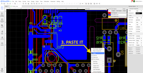


 The front (right side of the image) is 12mm in height and thinned as much as possible.


 This time, the PCB is inserted from the top side of the case, so it is changed to a flat shape so as not to interfere.


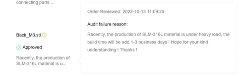


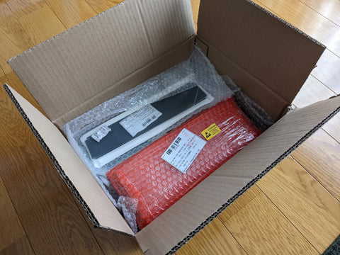


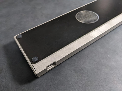


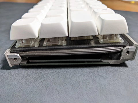


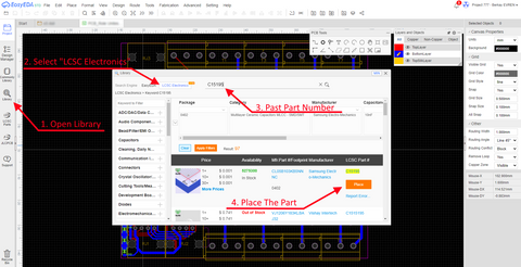


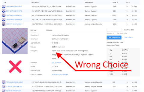


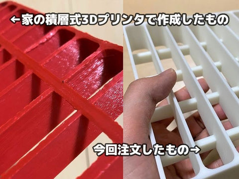


 Offer low prices and good profit margin to customers
 Reducing human error consequences