JLCPCB : Advanced PCB Design Techniques for High-Speed Signal Integrity
Introduction
Advanced PCB design techniques for high-speed signal integrity are critical for ensuring the reliable operation of electronic devices. One of the key considerations in designing high-speed circuits is controlling the transmission of high-frequency signals on the PCB. This is where JLCPCB play a vital role in providing advanced PCB design techniques to enhance signal integrity.
Differential Signaling
One of the most important advanced PCB design techniques for high-speed signal integrity is the use of differential signaling. This involves transmitting signals on a pair of conductors, rather than a single conductor. This technique helps to reduce the effects of electromagnetic interference (EMI) and crosstalk, which can cause signal distortion and loss of data. You can use EasyEDA PCB design software to create differential signaling pathways that optimize signal integrity. For example, a common differential signaling standard used in high-speed applications is LVDS (Low Voltage Differential Signaling), which uses a pair of signal lines to transmit data at speeds of up to 1.25 Gbps.

Controlled Impedance Transmission Lines
Another important technique for high-speed signal integrity is the use of controlled impedance transmission lines. These lines are designed to have a specific impedance value that helps to ensure the integrity of high-frequency signals as they travel through the PCB. PCB manufacturers use advanced simulation tools to design controlled impedance transmission lines that match the specific requirements of a given circuit. For example, a common controlled impedance transmission line used in high-speed applications is a microstrip, which is a type of transmission line that uses a trace on the surface of the PCB to transmit the signal. The width and thickness of the trace are carefully controlled by the PCB manufacturer to achieve the desired impedance value. The standard road thickness of JLCPCB is 1oz.
Length Matching
Length matching is crucial for maintaining signal integrity in high-speed applications because it minimizes the effects of signal skew. Signal skew is the difference in arrival times of different signals at a destination. When the length of the traces is not matched, the signals will arrive at different times, which can cause errors and reduce performance. In high-speed applications, such as DDR memory or high-speed serial links, the signal skew can be particularly problematic.
You can see an example of Lengt Matching in the image below.

Advanced PCB Materials
Another important aspect of PCB design for high-speed signal integrity is the use of advanced PCB materials. PCB manufacturers have a wide range of materials at their disposal, each with their own unique properties and characteristics that can affect signal integrity. Some of the advanced PCB materials that are commonly used include:
Low Loss Materials: PCB manufacturers may use low loss materials such as PTFE (Teflon) and Rogers for high-frequency applications. These materials have a low dielectric constant, which helps to reduce signal loss and improve signal integrity.
High-Speed Materials: PCB manufacturers may use high-speed materials such as Taconic and Arlon for high-speed digital applications. These materials have a high dielectric constant, which helps to reduce the effects of crosstalk and improve signal integrity.
Thermal Management Materials: PCB manufacturers may use thermal management materials such as metal core PCBs and ceramic substrates to manage the heat generated by high-speed circuits. These materials can help to improve the performance of high-speed circuits by reducing the effects of thermal expansion and contraction on signal integrity.
Specialty Materials: PCB manufacturers may use specialty materials such as high-frequency laminates, thermal interface materials, and high-frequency bonding materials to improve the performance of high-speed circuits.
By using advanced PCB materials, PCB manufacturers can help to ensure that high-speed circuits perform at their best. These materials can help to reduce signal loss and improve signal integrity, making them an essential part of PCB design for high-speed applications.
The use of advanced materials is also an important technique for high-speed signal integrity. PCB manufacturers use materials such as high-frequency laminates, which have a low dielectric constant and low dissipation factor, to reduce signal loss and improve the performance of high-speed circuits. In addition, can be use special laminates that include embedded passive components such as capacitors and resistors, which can further improve signal integrity. For example, may useble a laminate with an embedded capacitor to reduce the effects of power supply noise on high-frequency signals. For a good high-speed signal integrity, you can choose JLCPCB.
Power and Ground Planes
Another advanced PCB design technique that can use to enhance signal integrity is the use of power and ground planes. These planes provide a low-impedance return path for high-frequency signals, which helps to reduce the effects of ground bounce and power supply noise. You can use JLCPCB's EasyEDA PCB design tool to optimize the placement and layout of power and ground planes to minimize signal loss and distortion. JLCPCB use split plane layer, in which the top and bottom planes are separated by a thin dielectric layer, to reduce the effects of crosstalk between the power and ground planes.

Advanced PCB Manufacturing Techniques
In addition to advanced PCB design techniques, PCB manufacturers also use advanced PCB manufacturing techniques to enhance signal integrity. Some of the advanced PCB manufacturing techniques that are commonly used include:
Laser Drilling: PCB manufacturers may use laser drilling techniques to drill small, precise holes in PCBs.
Microvia Technology: PCB manufacturers may use microvia technology to create small, high-density vias on PCBs.
Through-Silicon Vias: PCB manufacturers may use through-silicon vias (TSVs) to create high-density interconnections between multiple layers of silicon.
Advanced Soldering Techniques: PCB manufacturers may use advanced soldering techniques such as reflow soldering and wave soldering to improve the performance of high-speed circuits.
These techniques can help to improve the performance of high-speed circuits by reducing the effects of crosstalk and improving signal integrity.
In conclusion, PCB manufacturers play a crucial role in ensuring high-speed signal integrity by providing advanced PCB design techniques, advanced PCB materials, and advanced PCB manufacturing techniques. These techniques and materials can help to reduce signal loss and improve signal integrity, making them essential for high-speed electronic devices. By working closely with PCB manufacturers, electronic device manufacturers can ensure that their high-speed circuits perform at their best. You can easily contact the JLCPCB team with live support.
Additional Considerations for PCB Manufacturers & Designers
When designing and manufacturing PCBs for high-speed signal integrity applications, there are a few additional considerations you should keep in mind.
PCB Layout: You should pay special attention to the layout of high-speed circuits to minimize the effects of crosstalk and EMI. This can include using techniques such as differential pair routing, controlled impedance routing, and via stitching to ensure that high-frequency signals are routed efficiently on the PCB.
PCB Materials: JLCPCB use advanced materials that are optimized for high-speed signal integrity applications. These materials may include low-loss dielectrics, low-loss laminates, and high-frequency metal substrates. You cannot pay attention to these in handmade circuits. For this reason, you can choose JLCPCB, where you can produce very fast and affordable PCB prototyping.
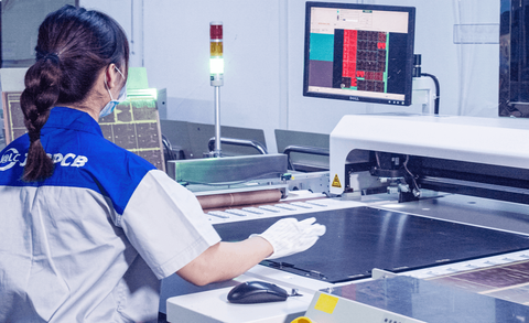
PCB Testing: JLCPCB use advanced testing and analysis techniques to ensure that high-speed circuits perform at their best. This can include techniques such as time-domain reflectometry (TDR) and frequency-domain reflectometry (FDR) to measure the performance of transmission lines and detect signal integrity issues.
PCB Assembly: JLCPCB also pay attention to the assembly process for high-speed signal integrity applications. This can include using advanced soldering techniques, such as reflow soldering, and ensuring that components are placed in the correct locations to minimize the effects of crosstalk and EMI.
PCB Quality Control: PCB manufacturers should also have a robust quality control process in place to ensure that high-speed signal integrity PCBs are manufactured to the highest standards. This can include regular testing and inspection of PCBs to ensure that they meet the required specifications and performance standards. In terms of quality control, your PCB is safe at JLCPCB. Have peace of mind.
By keeping these additional considerations in mind, JLCPCB can help to ensure that high-speed signal integrity PCBs are designed and manufactured to the highest standards.

Conclusion
In summary, advanced PCB design techniques for high-speed signal integrity are crucial for ensuring the reliable operation of electronic devices. JLCPCB play a vital role in providing these techniques by using state-of-the-art design software, advanced simulation tools, and specialized materials to optimize signal integrity.
By using these techniques and considering additional factors such as PCB materials, testing, assembly and quality control JLCPCB can help to ensure that high-speed circuits perform at their best for you.
You can also follow Project 777 - Berkay EVREN - YouTube channel, which is the main sponsor of JLCPCB, for such tips and detailed design videos with EasyEDA.
JLCPCB Part-Time Engineer / Berkay EVREN